Short Test of CM501 RT FAE Andrew Lin Function Introduction
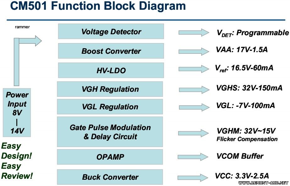
CM501 Function Block Diagram
V ref : 16.5V-60mA VGHM: 32V~15V Flicker Compensation VCOM Buffer Power
Input
8V
|
14V Gate Pulse Modulation
& Delay Circuit
HV-LDO
OPAMP
Easy Design!Easy Review!V DET : Programmable VAA: 17V-1.5A Voltage Detector
Boost Converter
VGH Regulation VGHS: 32V-150mA VGL Regulation VGL: -7V-100mA VCC: 3.3V-2.5A
Buck Converter
Power Sequence Control
Feature of Boost Converter
Efficiency(%) vs. Load Current(A) 10V/18V,12V/18V,14V/18V
70
75
80
85
9095
100
00.51
1.52Load Current(A)E f f i c i e n c y (%)VIN=10V VIN=12V VIN=14V
•Programmable Current Limitation •Output OCP/SCP/UVP/OVP •1% Deviation of FB reference •Internal Soft-Start Available
Boost Output Voltage(V) vs. Load Current(A)
17.2
17.25
17.3
17.3517.4
17.45
00.51
1.52Load Current(A)O u t p u t V o l t a g e (V )VIN=10V VIN=12V VIN=14V
Feature of Buck Converter
•Internal Compensation •Internal Soft-Start •1% Deviation of FB reference •Output OCP/SCP/UVP
BUCK Efficiency(%) vs. Load Current(A)
50
55
60
65
70
758085
90
95
00.51
1.52Load Current(A)E f f i c i e n c y (%)VIN=8V VIN=10V VIN=12V VIN=14V
BUCK Output Voltage(V) vs. Load Current(A)
3.196
3.206
3.216
3.226
3.2363.2463.2563.266
3.276
00.51
1.52Load Current(A)O u t p u t V o l t a g e (V )VIN=8V VIN=10V VIN=12V VIN=14V
Feature of VGH/VGL Regulation
•Driving ability up to
200mA of loading.•Driving ability up to 200mA of loading.
Output Voltage(V) vs. Load Current(A)
22
22.5
23
23.52424.5
25
00.050.1
0.150.2Load Current(A)O u t p u t V o l t a g e (V )VIN=8V VIN=10V VIN=12V VIN=14V
Feature of Gamma Reference
•0.5% Deviation of FB reference
•Good load regulation
Output Voltage(V) vs. Load Current(A)
15.061
15.0615
15.06215.062515.063
00.010.020.030.040.050.06
Load Current(A)
O u t p u t V o l t a g e (V )LDO_O
Protection Function of CM501
CM501 Protection Function
•VIN Undervoltage Lockout (UVLO)
•To avoid misoperation of the device at low input voltage
•The device is shut down when UVLO is occurred
•All power MOSFETs are turned-off in the lockout state
•VOUT Undervoltage Protection (UVP)
•To avoid output abnormal low, the device sets a fault latch when
the output is lower than the respective fault-detection threshold for a continuous duration time
•The output is shut down when the fault latch is occurred
•Once the fault condition is removed, cycle VIN to clear the fault
latch
CM501 Protection Function
•VOUT Short-Circuit Protection (SCP)
•The feature prevents potentially uncontrolled inductor current if VOUT is overloaded or shorted to ground •The output is shut down when the fault latch is occurred •Once the fault condition is removed, cycle VIN to clear the fault latch
•Over Current Protection (OCP)
•To limit the inductor current, the device has a cycle-by-cycle current limit
•The MOS switch is turned off when OCP is occurred.
CM501 Protection Function
•VOUT Overvoltage Protection (OVP)
•To protect Boost switch in case the feedback is floating or shorted to ground
•The MOS switch is turned off when OVP is occurred and the
converter continues to operate when VOUT falls below the
overvoltage threshold
•Thermal Shutdown (OTP)
•To prevent damage caused by excessive heat and power
dissipation
•The device is shut down when OTP is occurred
•Once the device cools down, cycle VIN to clear the fault latch
CM501 SCP Function
S R Q Q UVLO +
-
FB 0.5V +
-
FBP 0.5V +
-
0.85V FBN Timer w/o delay SCPB LatchB To shut down all outputs except VL and REF Timer w/o delay SCP SCPP SCPN S R Q Q Latch To shut down all outputs except VL, REF and step-down regulator +-
FBB 0.5V
UVLO +
-
ADJ 0.5V SCPL +
-OPOTP
Vref*k2VBE2OTP +
-
Vref*k1VBE1
CM501 UVP Function
Short Condition of VDA
Background
•Part: CM501-RT
•Test Condition:
•VIN=12V/VSA=17.5V/VDD=3.3V
•VSA: Node before PMOS; VDA: Node after PMOS.•Boost
•Short to GND while power-on
•Short to GND after operation
•Short to GND and aging for 4 hours
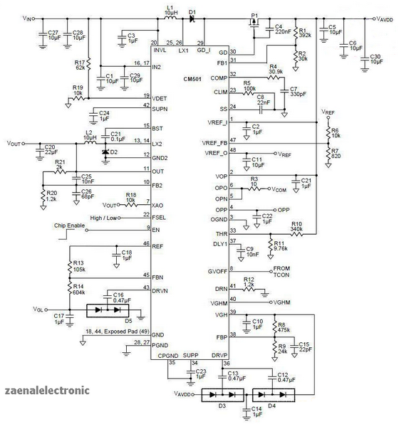
Application Circuit
Boost: Short to GND while Power On
•Result: Boost converter turns PMOS off and shut down the PMU. But the converter restarts after 200ms. CH1: VIN CH2: EN
CH3: VSA CH1: VDA CH2: EN CH3: VSA
Boost: Short to GND after Operation
•Result: Boost converter turns PMOS off. But the converter restarts after 200ms. CH1: VDA CH2: VSA
CH3: EN
Explanation of VDA short condition CH1: VSA
CH2: GD
CH3: EN
CH4: VDD
EN restarts and GD starts turning on the PMOS.PMOS is
ON but
short
current
makes VIN
drop.
UVLO makes BUCK be
off and EN falls to VIL.
BOOST stops action.
GD turns off PMOS.
BUCK UVP needs 50ms.
PMOS blocked
short condition.
And Vin rised.
BUCK works
again.
Short Test with/without Miller Capacitor
With Capacitor
Without
Capacitor
Vin=12V/3A
Power On Operation
Power Calculation
15ms I_D V_DS
2.2A
1.7A
3.75ms
7.5V
∫=⋅=W Idt V T
Power 02.11Period=200ms
Result and Discussion
•BOOST converter short to GND while Powering On or Operation.
•The fault protection will turn off the PMOS. But EN will restart after 200ms. Because the VIN falls into UVLO and BUCK restarts the power after VIN rises.
•After aging test for 4 hours under short condition, the PMU and PMOS both are normal for operation.
System Solution of CM501-RT VDA Short Test
Background
•Part: CM501-RT
•
Test Condition:
•
VIN=12V/
VSA=17.5V•VSA: Node before PMOS; VDA: Node after PMOS.•Find the solution of application circuit to avoid PMOS damaging while short.
•Short Test of Boost
•Short to GND while power-on
•Short to GND after operation
Application Circuit of Improvement
Short VDA to GND while power-on •D_S was on due to
VDA short. CH1: EN
CH2: VDA
CH3: VSA
CH4: I_VDA
Short VDA to GND after operation •D_S was on due to
VDA short.
CH1: EN
CH2: VDA
CH3: VSA CH1: EN CH2: GD CH3: VSA
Result and Discussion
•Shottky Diode, D_S pulled down the power on/off signal while VDA is short to GND.
http://www.doczj.com/doc/a83f093667ec102de2bd8963-3.html